
SMT vs THT PCB Assembly: Which Does Your Board Need?
Surface-mount or through-hole? A practical comparison of both assembly methods and when to use each.
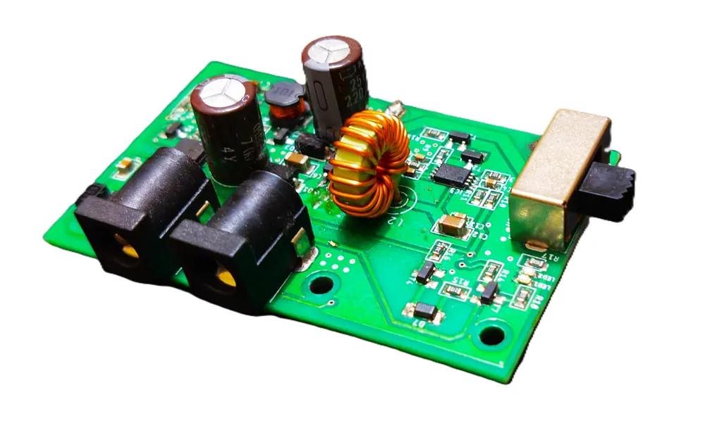
Design for manufacturability (DFM) means designing a board so it can be fabricated, assembled and tested reliably. Most delays and respins come from small issues that a quick review would have caught. Use this checklist before you send Gerber files to any fabricator or assembler. Exact limits vary by manufacturer, so always compare your design against the capability sheet of the shop that will build it.
Export all copper layers, solder mask, silkscreen, board outline and drill files from the same design revision. Open them in a Gerber viewer and confirm that nothing is missing or mirrored.
Check that your minimum trace width and spacing are within the fabricator’s capability for your copper weight. Tighter rules usually cost more and reduce yield.
Each via and hole needs enough copper ring around the drill after tolerances. Very small drills and thin rings are a common cause of rejected or unreliable boards.
Use standard through vias unless you really need blind or buried vias, which add process steps and cost. Avoid placing vias directly in component pads unless they are filled or capped.
Keep copper and components away from the board edge and from routed slots so that cutting or depanelising does not damage them.
Make sure solder mask openings are correct for each pad and that silkscreen text does not overlap pads. Very thin mask slivers between fine-pitch pads may not survive fabrication.
Leave enough room between parts for placement, soldering and inspection. Aligning similar components in the same orientation speeds up assembly and makes visual inspection easier.
Compare each footprint with the manufacturer’s datasheet drawing. A wrong pad size or pin 1 position is one of the most expensive mistakes to find after boards are built.
Add fiducial marks so placement machines can align accurately, and agree the panel layout with your assembler if you are ordering more than a few boards.
Use thermal relief on pads connected to large copper areas so they solder properly, and check that power components have enough copper or heat sinking.
Make sure every reference designator in the BOM exists on the board and that polarised parts (diodes, electrolytic capacitors, connectors) have clear polarity markings.
Add test points for power rails, key signals and programming or debug connectors. Access to these points saves hours during bring-up and makes production testing possible.
If you do not have a design yet, our product design and engineering team can take you from requirements to a manufacturable layout. When your files are ready, see what to send for an assembly quote or request PCB fabrication.
Surface-mount or through-hole? A practical comparison of both assembly methods and when to use each.
What to send for a fast, accurate PCBA quote and the mistakes that cause delays.
The steps from first idea to a tested prototype board, and where projects usually slip.
Tell us about your PCB, IoT or electronics project. Our engineering team will review your requirement and reply within 1 business day.